Modification of Star front end electronics for negative input
For comments or questions, please contact Madhu Dixit
We increased the quiescent output level of the STAR front end board charge-sensitive SAS preamplifier outputs from about 1.6 to 1.9V to allow for a larger dynamic range for the negative-going signals expected from, e.g., TPC pads. On the recomendation of Fred Bieser, this was done by decreasing two output stage bias resistors R38, R47 from 75K to 47K Ohms, the maximum permissible while staying within chip heat dissipation limits. Given the 16mV/fC gain of this IC, this would represent a maximum input charge of about 1.2pC for negative charge inputs.
We could still not utilize the full 10-bit digitizing range of the following ADC as its digitized output pedestal was at (allowing for the above new analog input level) about 200 to 250 counts.
With an additional circuit modification to vary the Vref voltage used by summing operational amplifiers in the SCA/ADC IC, one can adjust the pedestal count level even to the full 1024 digitizing range of the ADC. In practice one would set this count level to about 800 to allow for recording of pulse overshoot in the positive direction.
The circuit change involves a few, reversible changes to the STAR PCB. With reference to the Front End Electronic schematic (fee_e.pdf):
- a. Cutting first trace: between R100 (432 Ohms) and a via located between
bottom of R100 and R99 (2.21K Ohms).
b. Cutting of second trace: between top end of R99 (2.21k Ohms) and C100 (.01mF) filter capacitor (this node is located near pin 63 of nearby ADC IC).
The above disconnects the potential Vref of the reference divider chain from the Vref inputs, pins 49 and 79 of each of the two SCA/ADC-3 ICs.
- Wire jumper: from bottom of R100 to top of R99. This reconnects the
reference divider chain to provide the potential Vcap-bot as before.
- Jumper wire: from pin 1 (spare) of J3 to analog ground at bottom of R88
(2.21K Ohms), at node of this resistor and nearby 4.7 Ohm resistor (R79?).
This provides a ground for the Vref potentiometer to be installed on socket
J3.
- Wiring of small trimpot or fixed SMD resistors): to a header (Samtec
#TFM-105-S-D), wire such that trimpot terminals 1, 2 (wiper), 3 are connected
to terminals 2, 1 and 5 of J3. Pin 5 of this socket, labelled OP_AMP_Vref is
the connection to the Vref inputs on the two SCA/ADC ICs. Pin 2 on this socket
is the reference potential ADC_RAMP_TOP (3.41V) which allows one to select,
via trimpot adjust, any Vref from 3.41V to ground, i.e., the whole conversion
range of the ADCs. Pin 1 of J3 is connected to reference chain ground bottom
of R88 (2.21K Ohm) as described in step 3 above.
Plots
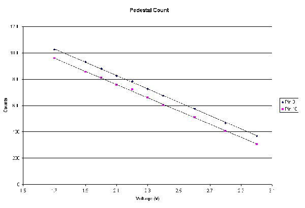
After the modifications, Vref can be adjusted with the trimpot. The following graph shows the relationship between Vref and pedestal count level. The plot shows only pins 0 and 10, but pins 0 through 8 produce nearly identical plots and pins 9 through 15 produce nearly identical plots. The small difference in count level between the two sets of pins is still under investigation.
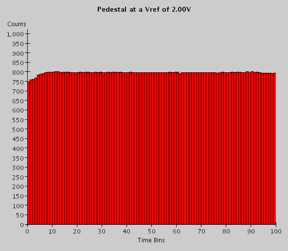
The following plot shows the quiescent count level with Vref set to approximately 2.00 volts.
Last updated on October 23, 2002